")
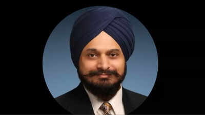
Dr Gurtej Sandhu stands among the most prolific inventors in modern semiconductor engineering, with 2,211 patents worldwide to his name, exceeding the 1,432 patents credited to Thomas Edison. Raised in Amritsar, he has built a career that bridges advanced research, corporate leadership and large-scale technology execution in the global memory chip industry. Now a citizen of the US, he continues to shape the direction of memory technology development.His innovations in memory chip process technologies power smartphones, digital cameras and cloud servers used daily across the world. Over more than three decades, he has remained closely involved in the evolution of semiconductor manufacturing, particularly in silicon CMOS processes that enable DRAM and NAND memory scaling.Education rooted in engineering and physicsDr Sandhu completed his MTech in electrical engineering from Indian Institute of Technology Delhi. He later earned a PhD in physics from the University of North Carolina at Chapel Hill in 1990. His academic training combined core electrical engineering with applied physics, forming the foundation for his later work in integrated circuit processing and semiconductor device fabrication.In recognition of his research accomplishments and corporate leadership, IIT Delhi conferred upon him the Distinguished Alumni Award. The honour acknowledged both his technical achievements and his role in advancing large-scale industrial research.Three decades at Micron TechnologyDr Sandhu has spent 35 years at Micron Technology, where he currently serves as Principal Fellow and Vice President. Based in Boise, Idaho, he leads the company’s end-to-end Si-to-Package R&D technology roadmaps. His responsibilities include identifying technology gaps, aligning cross-functional teams and directing engineering resources to develop scalable memory solutions.Before assuming his current role, he served as Senior Fellow and Vice President for over three decades. Throughout this period, he worked across multiple engineering and management positions, contributing to process innovations that are now embedded in mainstream semiconductor chip manufacturing worldwide.Leadership in semiconductor innovationDr Sandhu is recognised for pioneering several process technologies used in IC processing. He manages global project teams and collaborates with international research consortia, while also driving AI and ML-based methodologies to accelerate chip development cycles. His work focuses on enabling faster and more efficient scaling of complex memory technologies.He holds more than 1,300 US patents and over 2,200 patents globally, placing him among the leading inventors in the semiconductor field. A Fellow of Institute of Electrical and Electronics Engineers, he received the IEEE Andrew S. Grove Award in 2018 for contributions to silicon CMOS process technology enabling DRAM and NAND memory scaling.